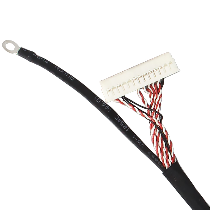
Since LVDS eliminates electromagnetic radiation, its noise is much lower than that of single ended signal radiation
This browser does not support the video element.

It is mainly designed to realize high-speed, low-power and low-noise point-to-point communication on 100 Ω medium with controllable balanced impedance. Like other differential signal standards, LVDS eliminates electromagnetic radiation, and its noise is much lower than that of single ended signal. At the same time, the external noise is coupled to the two lines as a common mode signal and is suppressed as a common mode signal, so its anti noise ability is much stronger than that of a single ended signal. In addition, the output of LVDS driver adopts current drive mode. Compared with voltage drive in other differential signal standards, it reduces the return current of ground wire and eliminates surge current. Reducing the voltage swing (only ± 350mV, PECL is ± 800mv, RS-422 is 2V) enables LVDS to achieve the same data rate as PECL (>800mbps), and the power consumption is only one tenth of PECL.
The high speed, low power consumption and low noise characteristics of LVDS make it an ideal choice for backplane interconnection of telecommunications and network equipment, interconnection within the rack of 3G cellular telephone base stations, digital video interfaces and other applications. In addition to the above advantages, LVDS serializer and deserializer also save a lot of space and money for system design. Using this scheme, the interconnection density can be reduced by five times, and a lot of space and cost can be saved in 3G and other communication applications with a large number of boards.Using capacitors to realize AC coupling of LVDS data connection has many benefits, such as level conversion, removing common mode errors and avoiding input voltage faults. This paper not only introduces the appropriate selection of capacitors, but also provides guidance for the topology of and terminals. At the same time, it also discusses the problem of common mode fault analysis.
LVDS logic input is one of many existing logic standards. As long as the signal source can provide sufficient amplitude for LVDS input, the typical value is differential 100mV Vp-p, and AC coupling can provide the required level conversion.
